MARKET OVERVIEW:
Global Plasma Dicing Systems for Semiconductor market is estimated to reach $149.2 Million by 2031; growing at a CAGR of 6.5% from 2024 to 2031.
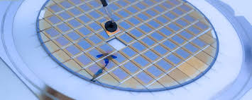
The Global Plasma Dicing Systems for Semiconductor market focuses on advanced wafer dicing technology, specifically plasma dicing which is considered cleaner and more efficient than traditional blade dicing. With the complexity and fragility of semiconductor chips increasing, there is a real need for non-destructive dicing techniques with high accuracy. Plasma dicing has emerged as an important technology to meet these needs.
Mechanical blade dicing tends to damage wafers easily and introduce defects, while plasma dicing uses chemical reactions to separate chips without cracking or contaminating them. Manufacturers in the semiconductor industry are shifting towards plasma etching to produce cleaner cuts, higher yields, and chips, especially as chips become smaller and more powerful. Additionally, plasma dicing allows for more versatile chip designs, facilitating new configurations and layouts not achievable with traditional dicing methods.
Plasma dicing systems are crucial as semiconductor fabrication moves towards larger wafer sizes, enabling handling of larger wafers without losing precision or quality. The market for Global Plasma Dicing Systems for Semiconductors is expected to grow due to the increasing demand for advanced packaging solutions, driven by technologies such as 5G, IoT, and artificial intelligence. As the industry progresses, plasma dicing is expected to become the standard in semiconductor production, particularly for accuracy and waste reduction.
Overall, the semiconductor industry is moving towards more efficient, accurate, and reliable manufacturing processes, with plasma dicing systems playing a key role in achieving these goals. The technology offers the ability to perform delicate dicing operations that will be crucial for next-generation semiconductor devices.

GROWTH FACTORS
The plasma dicing systems market in the semiconductor industry is expected to grow in the future due to the fast pace of technological advancement in semiconductor technology. Manufacturers are constantly pushing boundaries to create stronger and more efficient electronic devices, with plasma dicing systems playing a crucial role in this process by accurately cutting silicon wafers into smaller components. The increasing adoption of plasma dicing systems across various industries, driven by the demand for high-performance semiconductors in 5G, artificial intelligence, and the Internet of Things, is a major factor contributing to the market's growth.
However, the market also faces challenges, such as high initial costs that may deter smaller semiconductor manufacturers from using plasma dicing systems. The integration of these systems into existing manufacturing processes can also be complex and challenging for many businesses. Despite these obstacles, there are significant growth opportunities on the horizon, including the development of more cost-effective plasma dicing technologies that can broaden access to manufacturers and reduce operational costs.
With miniaturization becoming increasingly important in the electronics industry, there will be a growing demand for advanced plasma dicing systems that can provide precise and reliable cutting of wafers for smaller and more complex electronic devices. While high costs and integration challenges may pose obstacles, technological innovations and increased demand in the sector are expected to drive substantial growth in the global plasma dicing systems market for the semiconductor industry in the future.

MARKET SEGMENTATION
By Type
The market for plasma dicing systems in the semiconductor industry is evolving due to technological advancements and a growing demand for precision in manufacturing. It is divided into Batch Cutting Equipment and Single Cutting Equipment, each playing a distinct role in semiconductor production processes. In 2023, Batch Cutting Equipment is valued at $58. 3 million and is used for cutting up to three wafers simultaneously, boosting productivity in high-volume production. Meanwhile, Single Cutting Equipment, worth $32. 8 million in 2023, is designed for cutting single wafers with a focus on accuracy and flexibility in processing.
Batch Cutting Equipment is crucial for large-scale manufacturing due to its efficiency and cost-saving benefits, while Single Cutting Equipment is essential for niche markets requiring high-quality detailed processing. In the future, both types of equipment are expected to continue growing as Batch Cutting Equipment will cater to high-volume production needs, while Single Cutting Equipment will be used more in specialized fields that require precision. Advances in semiconductor technology will drive innovation in both types of equipment to meet evolving industry demands.
By Mobility
The Global Plasma Dicing Systems for Semiconductor market is progressing due to advancing technology. There are two main types of systems: Portable and Fixed. Portable systems are flexible and useful for mobility, enabling accurate dicing functions in various settings. The demand for portable systems is driven by the need for adaptability in semiconductor production as technology advances. These systems are likely to evolve to address specific industry needs over time.
Fixed Plasma Dicing Systems are designed for mass production within established facilities. They offer stability and consistent performance, important for high-volume production. With increasing demand for semiconductors, fixed systems will play a crucial role in ensuring efficient and reliable production processes. Both types of systems are expected to evolve in response to industry demands and technological advancements.
The development of Global Plasma Dicing Systems for Semiconductor market will be influenced by technological advances and changes in manufacturing practices and demand patterns. Portable and fixed systems will need to adapt to remain competitive and meet the requirements of semiconductor manufacturers. The categorization of systems cater to different demands and ensure efficient semiconductor production with advancing technology.
By Application
The Global Plasma Dicing Systems for Semiconductor market is growing, especially in thin wafer and chip segmentation applications. Plasma dicing is vital in semiconductor manufacturing, allowing precise cutting through semiconductor material efficiently and with minimal damage. Thin wafers are increasingly used in advanced electronic devices, driving demand for plasma dicing systems to handle fragile wafers with high precision.
These systems are also important for chip segmentation, dividing semiconductor wafers into individual chips for various electronic applications. As semiconductor technology advances, the market for plasma dicing systems will continue to grow, driven by the need for more accurate and efficient dicing methods. This will lead to the development of new materials and techniques to improve plasma dicing systems for higher performance and smaller form factors in electronic devices.
Overall, the market for Global Plasma Dicing Systems for Semiconductors is set to expand as it plays a crucial role in meeting the demands of chip segmentation and thin-wafer processing in the ever-evolving semiconductor industry.
REGIONAL ANALYSIS
The global Plasma Dicing Systems market is divided into five major regions based on its use in the semiconductor industry: North America, Europe, Asia-Pacific, South America, and Middle East & Africa.
North America, which includes the United States, Canada, and Mexico, is a key region in the semiconductor market. The U. S. and Canada have leading semiconductor manufacturers and technological companies, driving demand for high-end Plasma Dicing Systems. Furthermore, the growing electronics industry in Mexico is expected to boost the regional market.
With ongoing technological advancements and investments in semiconductor research and development, North America is expected to continue being a significant market.

KEY INDUSTRY PLAYERS
The Global Plasma Dicing Systems for Semiconductors market has vast potential for growth due to advancements in technology and competition. Key leaders in the industry include KLA Corporation, Panasonic Connect Co. , Ltd. , Plasma-Therm LLC, Samco Inc. , DISCO Corporation, and SUMITOMO PRECISION PRODUCTS Co. , Ltd. Each of these companies is driving innovation in plasma dicing systems to expand the distribution of semiconductors into new markets.
KLA Corporation is known for its focus on precision and performance, offering advanced plasma dicing systems that provide exceptional accuracy for high-quality semiconductor production. Panasonic Connect Co. , Ltd. combines experience and innovation in its systems, aiming to become a major player in the semiconductor market. Plasma-Therm LLC’s flexible and efficient systems cover a wide range of semiconductor manufacturing needs, contributing to industry innovation. Samco Inc. specializes in high-performance plasma dicing systems with a focus on precision and process control to remain competitive in a rapidly changing market.
DISCO Corporation provides reliable plasma dicing solutions with an emphasis on system efficiency and performance improvements to meet future semiconductor manufacturing demands. SUMITOMO PRECISION PRODUCTS Co. , Ltd. offers cutting-edge plasma dicing systems with a commitment to high precision and reliability, positioning itself as a competitive force in the global semiconductor market. Overall, as these industry leaders continue to innovate, the market will evolve to prioritize efficiency, precision, and performance in semiconductor manufacturing.
REPORT SCOPE AND SEGMENTATION
|
Attributes |
Details |
|
Market Size By 2031 |
USD 149.2 Million |
|
Growth Rate |
CAGR of 6.5% |
|
Forecast period |
2024 - 2031 |
|
Report Pages |
250+ |
|
By Type |
|
|
By Mobility |
|
|
By Application |
|
|
By Region |
|
|
Key Market Players |
|


_page-000129.jpg)
_page-000131.jpg)
_page-000130.jpg)
_page-000128.jpg)

1.jpg)


 APAC:+91 7666513636


